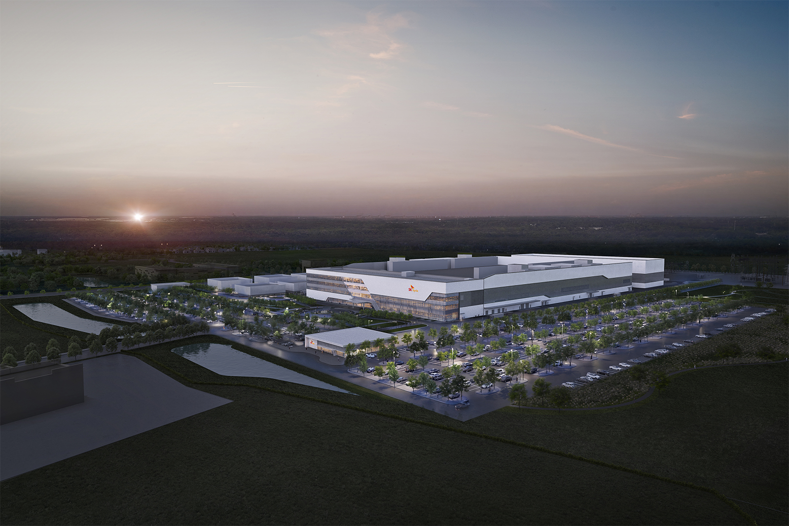
SK hynix has broken ground on its advanced memory-packaging facility in Indiana, moving an investment of more than $4 billion into construction as demand for high-bandwidth memory continues to expand around AI computing.
SK hynix held the groundbreaking ceremony in West Lafayette on 27 August local time. The company plans to open the facility’s cleanroom by October 2028 and begin mass production of next-generation HBM during the second half of 2029.
The Indiana operation will become SK hynix’s first HBM production base in the United States, although it will remain closely integrated with Korean manufacturing. Advanced wafers produced in South Korea will be shipped to Indiana for packaging and testing before completed products are supplied to customers in the US.
Approximately 1,000 people are expected to work at the site during commercial operation. SK hynix also estimates that construction and subsequent activity could create around 7,000 direct and indirect jobs, while more than 100 companies are being considered as suppliers of materials, components, and equipment.
The project addresses the increasingly important back end of semiconductor manufacturing. Advanced packaging combines or vertically stacks multiple chips within a package, allowing memory and processors to exchange data at far higher rates than would be practical if the devices were connected through conventional board-level interfaces.
HBM applies that principle to DRAM. Multiple memory dies are vertically interconnected to provide much greater data bandwidth, making the product particularly valuable alongside GPUs and other processors used for AI workloads.
Packaging those devices is considerably more complicated than placing a conventional memory die into a protective enclosure. The manufacturing sequence has to manage thin dies, dense electrical connections, stacking accuracy, bonding, materials behaviour, thermal performance, inspection, and testing while preserving acceptable yield across a product assembled from several high-value semiconductor components.
That difficulty increases as manufacturers add more layers and reduce the spacing between connections. SK hynix is already developing technologies such as hybrid bonding, where copper connections can be made directly without conventional bumps, allowing denser interconnects and thinner stacked structures.
The Indiana investment therefore includes an Advanced Packaging R&D Testbed alongside commercial production. SK hynix says customers, universities, and suppliers will be able to develop packaging processes, fabricate prototypes, and validate performance before technologies progress towards larger-scale manufacturing.
Purdue University is central to that work. An R&D memorandum signed during the groundbreaking covers next-generation system integration and advanced packaging, extending the university relationship that formed part of the original investment proposal.
Locating development activity beside production can shorten the transfer from prototype process to qualified manufacturing line, although semiconductor equipment still has to pass extensive process development and yield learning before a laboratory result can operate reliably at commercial rate.
The US Department of Commerce awarded up to $458 million in direct CHIPS Act incentives to the project in December 2024 and made up to $500 million of loans available. At that point, SK hynix’s planned private investment was approximately $3.87 billion; the company now describes total expected expenditure as exceeding $4 billion.
The production timetable has evolved as the project has developed. Earlier federal material anticipated next-generation HBM production during the second half of 2028. SK hynix’s current construction programme instead targets cleanroom opening in October 2028 and mass production during the second half of 2029.
Those milestones describe different stages of semiconductor commissioning. Completing a cleanroom allows process equipment to be installed and connected, but production tools must then be calibrated, qualified, integrated into the manufacturing flow, and brought through yield improvement before commercial volumes are available.
The factory will also depend on Korean wafer output, so Indiana does not create a self-contained American HBM supply chain. Front-end memory fabrication remains one of the most capital-intensive and technically demanding stages of the process, and the new plant has been designed around continued trans-Pacific movement of wafers.
It does, however, add a major advanced-packaging stage in the US. Packaging has become a recognised supply constraint as AI processors consume growing quantities of HBM and semiconductor companies increasingly combine memory, logic, and other functions in more tightly integrated systems.
The distinction between front-end fabrication and packaging is also becoming less clear commercially. Traditional back-end operations were often treated as lower-value assembly work; HBM and other advanced packages now depend on equipment, materials, process development, and yield control that can be as strategically important as some wafer-level technologies.
SK hynix has already mapped a longer-term route towards tighter integration of memory, processors, and optical interconnects, which would place still greater pressure on packaging technologies to manage signal density, heat, and manufacturing yield.
The West Lafayette operation gives the company a site where some of that development can take place closer to major American AI customers. It also gives equipment and materials suppliers a reason to establish local technical support, inventory, or applications engineering even if their underlying manufacturing remains elsewhere.
Supplier localisation will be gradual. Semiconductor plants depend on highly specialised global businesses for process tools, chemicals, gases, substrates, materials, software, components, and maintenance expertise, and a single US facility will not duplicate that ecosystem quickly.
The new plant instead adds another geographic stage to SK hynix’s existing manufacturing network. Korean fabs will continue to make the advanced wafers while Indiana specialises in converting those wafers into finished HBM packages through increasingly sophisticated assembly and test processes.
With the groundbreaking completed, the next milestones are less ceremonial: civil construction, cleanroom completion, equipment installation, process qualification, recruitment, and yield ramp. The AI market may be setting the demand case, but Indiana will reach useful production through the same painstaking manufacturing sequence that governs every semiconductor factory.