Kioxia and Sandisk are planning more than $31 billion of Japanese flash-memory investment through 2032, extending a 25-year manufacturing partnership as demand for high-capacity storage drives another semiconductor expansion cycle.
Kioxia and Sandisk put the anticipated investment at approximately ¥5 trillion, with expenditure dependent on continued Japanese government support. The programme will cover production infrastructure and technology at Kioxia’s Yokkaichi and Kitakami plants, alongside related facilities required to increase output of advanced three-dimensional NAND flash memory.
The two companies have invested more than $50 billion, or approximately ¥9 trillion, in Japan during their long-running joint venture. Their arrangement combines technology development and wafer manufacturing, allowing both businesses to share the capital required for successive generations of flash memory while selling products through separate commercial operations.
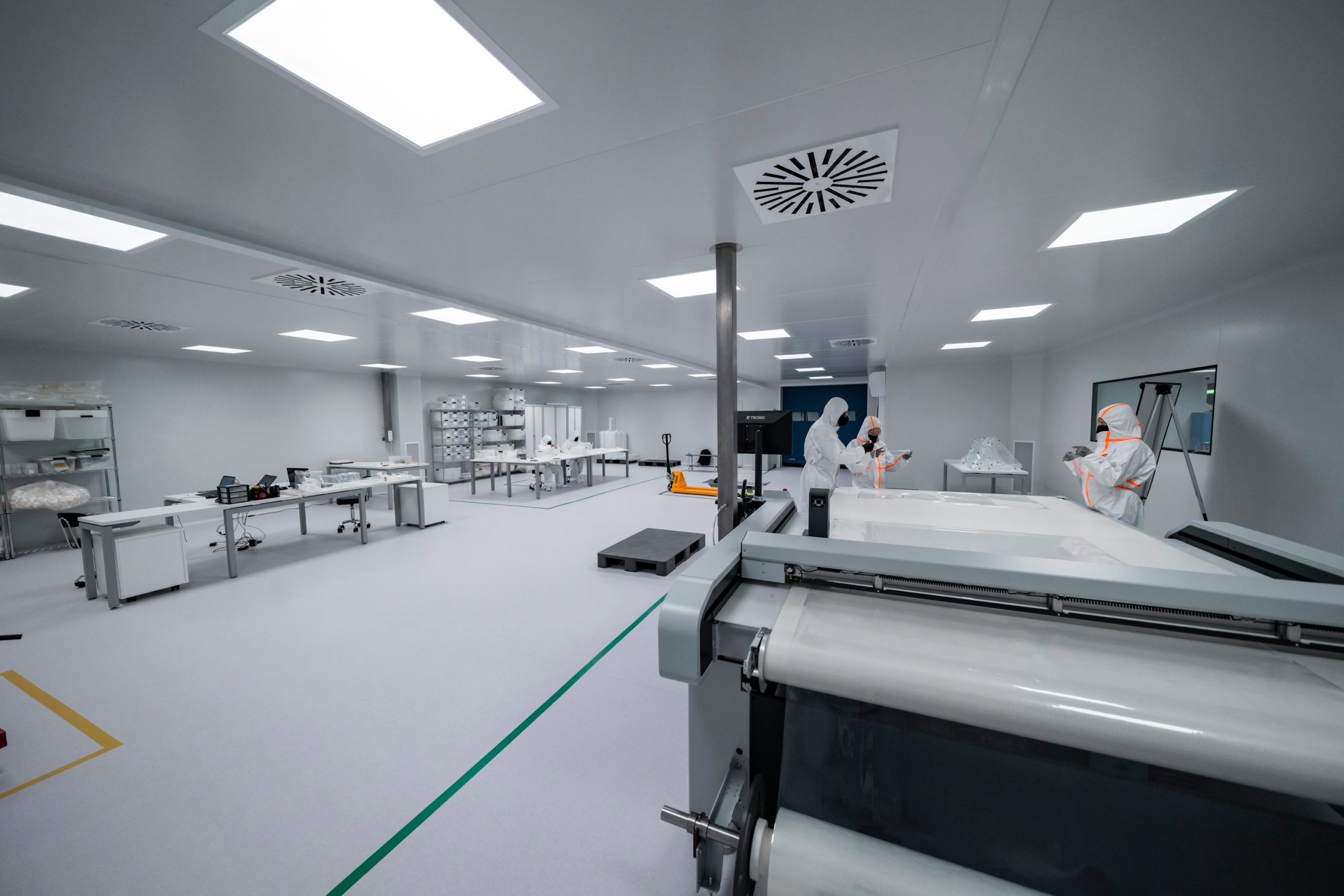
The latest commitment gives that model a much longer investment horizon. Semiconductor factories need capital decisions years before additional output reaches customers because cleanrooms, utilities, process equipment, qualification, and yield improvement all have to be completed before a new production line can contribute meaningful volume.
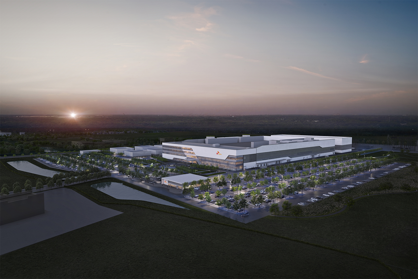
Kioxia separately confirmed on 27 August that it has started preparing land for a third manufacturing building at its Kitakami plant in Iwate Prefecture. Fab3 will be constructed south of Fab2, with operations targeted to begin during fiscal 2029.
The company has not yet fixed the detailed construction or equipment-investment schedule for Fab3, saying those decisions will depend on market conditions. Government support is also a condition of investment in the new building, leaving the pace of equipment installation open even though site preparation has started.
That flexibility reflects the volatile economics of memory production. NAND manufacturers invest against long-term growth in stored data, but selling prices can move sharply when new capacity, customer inventories, or weaker device demand leave the market temporarily oversupplied.
A semiconductor shell can therefore be completed without immediately being fitted out to maximum capacity. Equipment orders and wafer starts can be phased against demand, giving manufacturers more control over how quickly new cleanroom space translates into saleable output.
Kitakami is already progressing through one such production ramp. Kioxia and Sandisk began production of their tenth-generation 3D flash technology at Fab2 in July, following the building’s opening in September 2025.
The tenth-generation process uses CMOS directly Bonded to Array technology, which manufactures the memory-cell array and peripheral CMOS circuitry separately before bonding them together. Kioxia says the approach supports higher performance and density while allowing the two parts of the device to be optimised with greater independence.
Fab2 has been designed with earthquake-absorbing construction, energy-saving manufacturing equipment, and AI-assisted production systems. Those systems sit inside an industry where equipment data, inspection results, process conditions, and yield information are collected continuously across thousands of manufacturing steps.
Yield is critical because increasing the number of memory layers does not automatically increase commercial output if more devices fail electrical or quality tests. Deposition, etching, bonding, metrology, thermal processing, and contamination control all become more demanding as manufacturers add density to increasingly complex three-dimensional structures.
Kioxia and Sandisk consequently describe their investment plans in terms of multi-year bit growth rather than wafer capacity alone. More advanced process generations can increase the quantity of usable memory produced from each wafer, while additional buildings create the physical capacity needed to install more manufacturing equipment.
The commercial demand behind those investments is also changing. Enterprise storage is taking a larger share of NAND production as AI infrastructure moves beyond model training into inference systems that require large quantities of persistent, high-performance storage.
Enterprise SSDs accounted for 48% of global NAND bits shipped in the second quarter of 2026, up from 26% a year earlier. That shift leaves traditional PC, smartphone, automotive, embedded, and consumer-storage markets competing with data-centre customers for an increasingly important share of industry output.
Enterprise products also carry different manufacturing and qualification requirements. High-capacity server storage has to deliver endurance, performance consistency, firmware stability, and predictable supply across long infrastructure deployment cycles, rather than simply maximise capacity at the lowest consumer price.
Kioxia and Sandisk extended their Yokkaichi joint venture agreement earlier this year through December 2034. The corresponding Kitakami arrangement is aligned to the same date, giving the companies a contractual period long enough to cover Fab3’s planned start-up and several subsequent process generations.
The investment also sits inside Japan’s wider attempt to secure more advanced semiconductor manufacturing. Public support is increasingly used across the US, Europe, Japan, South Korea, and other economies because fabs create demand for equipment, chemicals, gases, materials, construction, power infrastructure, and highly specialised technical work far beyond the company operating the cleanroom.
That does not insulate Kioxia and Sandisk from the memory cycle. A plan running to 2032 will cross several periods of stronger and weaker NAND pricing, and both companies have left themselves room to alter spending against market conditions.
Site preparation at Fab3 nevertheless gives the programme a physical starting point. The investment announcement is no longer solely a long-range capital intention: Kioxia is preparing another manufacturing building while Fab2 ramps a new process generation immediately alongside it.
How quickly Fab3 fills with equipment will provide the clearer measure of demand. Semiconductor factories are expensive buildings, but the lithography, deposition, etch, bonding, inspection, and other tools installed inside them account for much of the production capability that ultimately determines output.
Kioxia and Sandisk are therefore planning on two timescales at once — extending their manufacturing relationship into the 2030s while retaining enough flexibility to avoid filling new capacity faster than customers can absorb it. The $31 billion figure is substantial; the sequencing of that spending will be the more useful indicator of how confident the partners remain in flash-memory demand.