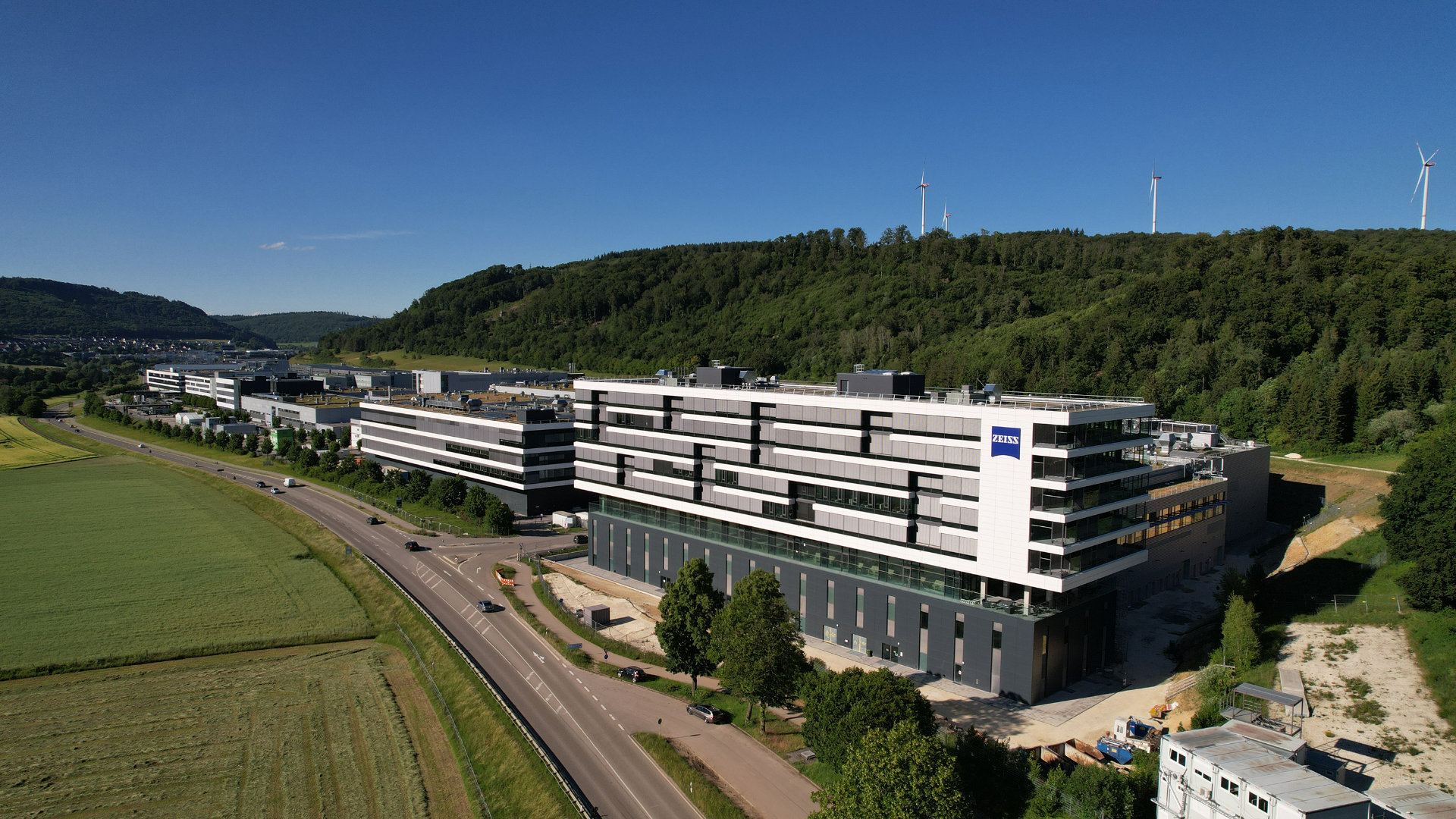
Zeiss Semiconductor Manufacturing Technology is adding approximately 25,000m² of production and production related space at its Oberkochen campus in Germany, expanding capacity for optical and metrology systems used in advanced semiconductor manufacturing.
Four years after construction began in May 2022, employees have moved into the first office building completed within the programme. Additional buildings will enter service progressively, supporting production, development, and technical operations across the company’s semiconductor equipment portfolio.
Oberkochen produces high precision optical systems for extreme ultraviolet lithography, including technology required for the next generation of High-NA EUV machines. Zeiss also develops equipment used in photomask production and repair, wafer inspection, defect analysis, metrology, and advanced semiconductor packaging.
EUV lithography directs light with a wavelength of 13.5 nanometres through a series of specialised mirrors, because conventional refractive lenses cannot operate effectively at that wavelength. Extremely small surface or coating errors can affect the pattern transferred onto a wafer, placing severe demands on materials, polishing, multilayer deposition, measurement, assembly, vacuum, and environmental stability.
The Oberkochen project forms part of a wider capacity programme spanning Zeiss sites in Germany and customer support operations internationally. Facilities and cleanroom capability have also been expanded in Wetzlar, Rossdorf, and Jena, while technical and service investments are being made closer to semiconductor manufacturers in Asia and the United States.
Qualified output follows construction slowly
Demand for EUV lithography has increased as chipmakers pursue smaller process nodes and more complex device structures. Zeiss is a critical supplier to ASML’s EUV systems, which means its ability to manufacture and qualify complete optical assemblies influences the number of scanners that can be delivered to wafer fabrication plants.
New floor area alone cannot remove that constraint. Specialist production equipment, environmental systems, metrology, trained personnel, process maturity, and cleanroom qualification must all be established before a building contributes reliable output. Construction may finish months or years before every process reaches its required yield and cycle time.
Many of the required operations depend on accumulated production knowledge that cannot be transferred through drawings alone. Engineers must understand how material condition, temperature, vibration, surface treatment, coating behaviour, contamination, and measurement uncertainty combine to influence final optical performance.
European semiconductor investment is increasing across several points in the manufacturing chain. Infineon’s new power semiconductor capacity in Dresden addresses demand for automotive, energy, and industrial devices, while Zeiss is expanding the equipment base needed to support more advanced wafer production.
Both investments illustrate the infrastructure required before semiconductor output begins. Clean utilities, stable electricity, water treatment, process gases, chemical handling, vibration control, automation, fire protection, and environmental monitoring must operate continuously, often within tolerances far tighter than those expected in general manufacturing.
Advanced packaging is creating another source of demand as manufacturers combine processors, memory, communications, and specialist accelerators within multi-die assemblies. This approach avoids producing every function on the most expensive process node, but increases the need for precise alignment, bonding, inspection, and defect analysis during packaging.
As more functionality is placed within one package, defects at interfaces can destroy the value of several otherwise usable dies. Inspection systems must identify faults without damaging the assembly or slowing production so severely that the package becomes uneconomic.
The concentration of EUV capability among a small number of suppliers remains a strategic vulnerability. Expansion at Oberkochen can increase output and resilience within Zeiss, although it also reinforces the dependence of leading edge semiconductor production on a highly specialised site whose processes cannot be substituted rapidly.
Recruitment and training will be as important as equipment installation. Precision optics, surface science, mechatronics, vacuum engineering, software, metrology, and semiconductor process knowledge must operate together, while much of the required competence develops through practical work over several years.
Zeiss intends the new capacity to support future generations of semiconductor technology alongside current platforms. Each building will contribute only when its equipment, processes, and workforce can produce assemblies that pass customer qualification consistently.
The expansion consequently represents a long manufacturing ramp rather than a single increase in nominal capacity. Semiconductor customers will judge its progress through qualified systems, delivery reliability, and shorter equipment lead times, not through the amount of completed floor space at Oberkochen.