NXP Semiconductors has broken ground on a major expansion of its assembly and test operation in Petaling Jaya, Malaysia, adding around 500,000 square feet of semiconductor production space. The automated facility is expected to begin ramping in the first quarter of 2028 and more than double output from the site when it reaches full operation.
The project will take the Malaysian facility to approximately 900,000 square feet of production space. NXP says the additional backend capacity will support its wider manufacturing network, including expected wafer output from the VSMC joint venture in Singapore and the ESMC joint venture in Dresden. The investment therefore forms part of a broader production architecture rather than an isolated factory expansion serving only local demand.
Assembly and test sits downstream of wafer fabrication but remains a critical semiconductor manufacturing stage. Processed wafers have to be separated into individual dies, packaged, connected electrically, tested, inspected, and prepared for shipment in forms capable of surviving production and operating reliably inside finished equipment. A shortage of backend capacity can consequently restrict semiconductor supply even where sufficient wafers are available upstream.
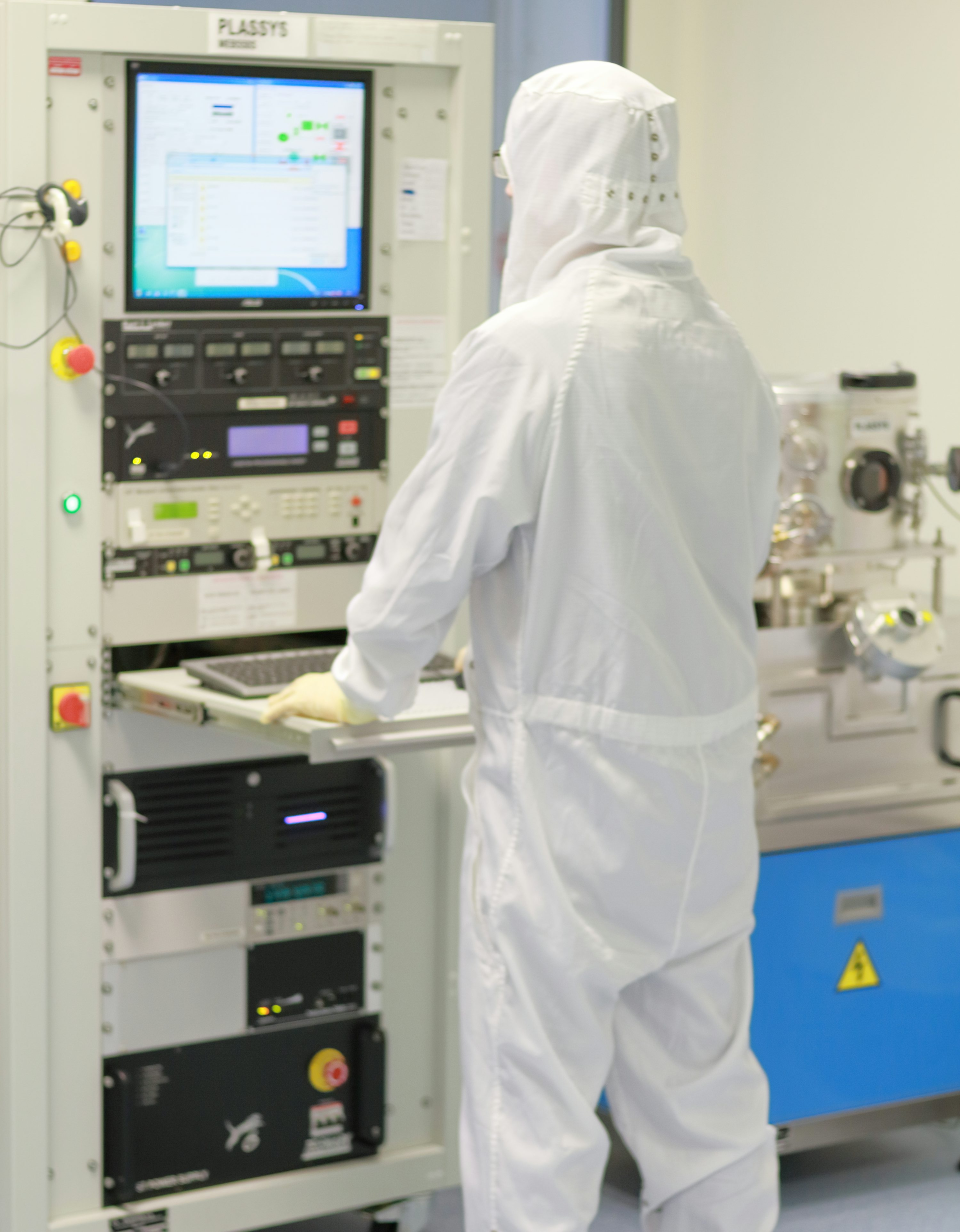
NXP’s expansion is designed as a highly automated smart factory using automated material-handling systems and advanced quality-management technologies. Material control is particularly important in semiconductor production because large numbers of lots, package types, recipes, test routes, and process stages have to move through equipment without losing identity or traceability. Automated handling reduces manual transport while allowing production systems to direct material according to equipment status, process requirements, and priority.
The quality-management layer is equally important. Semiconductor defects can originate in wafer fabrication, packaging, assembly, handling, contamination, mechanical damage, or electrical test, while many NXP devices are destined for automotive and industrial applications where field failures can be expensive. Production data therefore needs to connect test results with lot history, equipment, materials, and process conditions so abnormal trends can be isolated before they propagate through significant volumes.
NXP describes the Malaysian investment as part of a hybrid manufacturing strategy combining internal production with external partners. That approach allows a semiconductor supplier to vary where individual process stages are carried out while retaining more direct control over selected strategic capacity. The value of that flexibility became particularly visible during recent supply disruptions, when constrained manufacturing at one point in the chain could affect customers several stages downstream.
Greater internal assembly and test capacity does not make the supply chain self-contained. Semiconductor packaging relies on substrates, leadframes, mould compounds, chemicals, test equipment, handlers, connectors, and specialist production machinery supplied through international networks. The resilience benefit comes from increasing options and geographic balance rather than removing dependence on outside suppliers.
Malaysia already has a substantial semiconductor backend ecosystem, and NXP has manufactured there since 1972. That history provides access to an established workforce, suppliers, infrastructure, and technical knowledge base while avoiding the need to create an entirely new operating environment. The company is also working with Malaysian universities on engineering education and research as competition for semiconductor skills increases alongside manufacturing investment.
The links with VSMC and ESMC are particularly relevant because additional wafer-fabrication capacity creates downstream requirements that have to be planned years in advance. A front-end fab may represent the largest individual capital investment, but completed wafers still need suitable packaging and test capacity before devices can reach customers. Expanding Petaling Jaya ahead of expected output from those joint ventures reduces the risk of assembly and test becoming the next production constraint.
Automation should also allow the enlarged operation to absorb more output without requiring labour to scale directly with floor area. Automated transport, recipe management, equipment integration, statistical process control, and digital quality systems can increase throughput while reducing handling variation. Those technologies create their own dependencies on software, sensors, industrial networks, maintenance, and cybersecurity, meaning production continuity increasingly depends on the performance of both physical and digital infrastructure.
The Q1 2028 ramp gives NXP time to install equipment and qualify processes before the site approaches full output. Semiconductor factories cannot simply install machinery and begin shipping qualified devices at nameplate capacity. Individual package types, test programmes, materials, equipment sets, and customer requirements have to be validated, while yields need to stabilise sufficiently for the economics of the new capacity to work.
The scale of the Malaysian expansion is unusually clear: roughly half a million additional square feet, a total production footprint of about 900,000 square feet, and output expected to more than double at maturity. Groundbreaking starts the visible part of the project; equipment installation, process qualification, automation integration, and yield ramp will determine how quickly that floor space becomes usable semiconductor capacity.