Lam Research plans to invest more than US$3 billion over five years to expand its global semiconductor research and development laboratory network, with the company targeting an increase of more than 50% in experiment capacity.
The multi-site programme will add infrastructure and capabilities across laboratories in the United States, Asia, and Europe. Lam says its existing R&D network already supports more than one million experiments annually, making the proposed increase a substantial addition to process-development capacity rather than another conventional corporate research office.
The investment is intended to shorten the route from early materials and process research to equipment and recipes capable of being deployed in customer fabs. Lam operates specialised laboratories for foundational research, process-development facilities that move those ideas towards production readiness, and technology centres close to customers for qualification and validation.
Those stages are increasingly difficult to separate. Advanced semiconductor manufacturing depends on tightly coupled deposition, etch, cleaning, lithography, and packaging processes, so changes intended to improve one feature can create integration or defect problems elsewhere in the manufacturing flow.
More experiment capacity gives engineers additional room to investigate those interactions before a process reaches high-volume production. That matters particularly at advanced nodes, where relatively small variations in materials, dimensions, plasma conditions, or process sequence can affect yield across expensive wafers.
Lam says its laboratories operate as an integrated 24-hour network, sharing tools, data, and expertise between locations and time zones. In recent customer engagements, the company says that model has shortened process development by as much as 2.5 times.
The new investment is intended to increase the volume of work that can run through the network simultaneously. Rather than waiting for one site to complete an experiment before another group can begin its own work, engineering teams can use distributed facilities to develop different parts of a process flow in parallel.
The timing reflects the growing complexity of semiconductor devices built for artificial-intelligence workloads. Leading logic, high-bandwidth memory, advanced DRAM, and heterogeneous packaging require increasingly complex structures, tighter dimensional control, and new combinations of materials.
That pushes more development work towards the wafer-fabrication equipment supplier. Chip manufacturers cannot simply buy a deposition or etch tool and assume that it will deliver a finished device structure without extensive process development, integration, and qualification around the customer’s particular architecture.
Laboratory capacity therefore sits upstream of semiconductor manufacturing but remains directly connected to production ramps. Before a process recipe can be released to a fab, engineers need evidence that it can meet required uniformity, defect, throughput, reliability, and integration targets over repeated wafer runs.
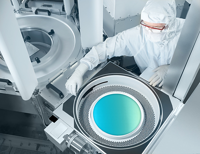
Lam’s US$3 billion plan should consequently be distinguished from investment in a semiconductor fabrication plant. The company supplies wafer-fabrication equipment rather than manufacturing chips itself, so the capital will expand R&D infrastructure, development tools, cleanroom capability, metrology, and supporting engineering rather than add a published wafer-per-month production capacity.
That distinction changes how the investment is measured. A chip fab ultimately demonstrates progress through installed wafer capacity and production yield, while an equipment supplier’s R&D estate is judged through process-development speed, qualified technologies, customer adoption, and the number of experiments engineers can complete.
Lam says its foundational-research facilities can compress weeks of experimental work into days in some cases. Process-development laboratories then bring engineering, product-development, and manufacturing teams together around the same equipment, while customer-proximate technology centres are used for final qualification work.
The geographic spread also has practical value. Semiconductor manufacturing is distributed across several major regions, while customers follow different technology roadmaps and fab schedules. Locating development facilities closer to those customers can reduce the time involved in moving wafers, hardware, and engineering teams between continents.
It does not remove geopolitical constraints. Export controls, trade restrictions, and national technology policies increasingly affect where advanced semiconductor equipment can be sold and supported, so a distributed laboratory network still operates inside a fragmented regulatory environment.
The expansion also creates a workforce requirement. More laboratories and equipment need process engineers, materials scientists, mechatronics specialists, equipment engineers, software staff, technicians, and cleanroom support. Physical tools can be ordered against a capital budget more quickly than experienced semiconductor-development teams can necessarily be recruited.
Lam has not published a site-by-site allocation of the US$3 billion or detailed construction schedules for each laboratory. It plans to begin expanding the network during 2026, leaving subsequent announcements to define where the largest additions will occur.
The programme nevertheless carries a measurable operational target: more than 50% additional experiment capacity across an estate already processing over one million experiments annually. New cleanroom space and installed tools will provide the physical evidence, but the industrial result will be whether process-development cycles shorten as device structures continue becoming more difficult to manufacture.