Fujifilm has started production at a new semiconductor-materials facility in Oita, Japan, tripling the site’s manufacturing capacity for post-CMP cleaners used during advanced chip fabrication.
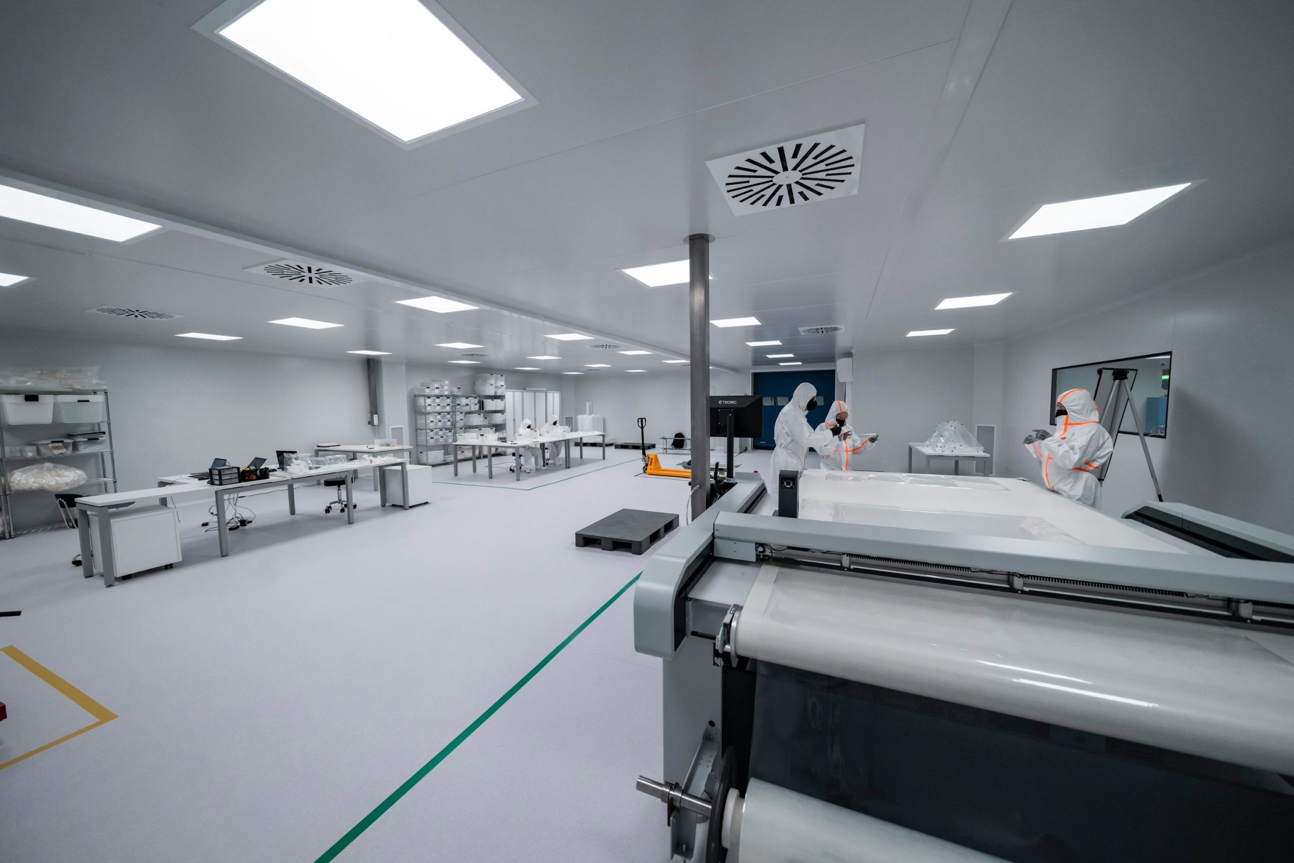
The four-storey building represents an investment of approximately ¥7 billion and provides around 3,600m² of floor area. It contains production and quality-inspection equipment alongside office space and began operating during August.
The plant is operated by Fujifilm Electronic Materials, the group company responsible for semiconductor process materials. Its immediate focus is high-purity cleaning chemistry used after chemical mechanical planarisation, or CMP, one of the repeated process stages involved in creating increasingly complex integrated circuits.
CMP combines chemical action with mechanical polishing to remove material from a wafer and create an extremely flat surface. Semiconductor structures are built through repeated deposition, patterning, etching, and polishing steps, and small variations in surface height become increasingly problematic as dimensions shrink and more layers are added.
Polishing leaves its own contamination problem. Residual slurry particles, metals, oils, and other process material must be removed without damaging the wafer surfaces or structures that have just been created. Post-CMP cleaners therefore have to remove unwanted material while remaining compatible with an increasingly complicated combination of metals, dielectrics, and other semiconductor materials.
That makes purity a production parameter rather than a marketing description. Trace contamination introduced by the cleaning chemical, storage vessel, pipework, pump, filter, filling equipment, or container can undermine the process the cleaner is intended to protect.
Fujifilm has equipped Oita with automated manufacturing and enhanced quality-evaluation capability as it increases volume. Scaling a semiconductor chemical process means maintaining the same impurity controls and formulation consistency across larger batches, more containers, and higher throughput.
The requirement becomes more stringent as device structures become more advanced. AI processors and other high-performance semiconductors use dense transistor structures, complex interconnects, and increasingly sophisticated packaging, creating more opportunities for particles or metallic contamination to damage yield.
Demand for cleaning materials therefore rises with more than the number of wafers entering a fab. Additional processing stages can increase chemical consumption per finished device, particularly where advanced structures require repeated planarisation and cleaning sequences.
Fujifilm expects sales of its post-CMP cleaner range to more than double by the 2030 financial year compared with 2024. The forecast remains a company target, but tripling Oita capacity gives the business manufacturing headroom if that demand materialises.
The investment forms part of a much larger semiconductor-materials expansion. Fujifilm has invested more than ¥100 billion in the activity over recent years and has expanded production across several regions and material categories.
Its portfolio includes CMP slurries, post-CMP cleaners, photoresists, polyimides, photolithography materials, high-purity chemicals, and other process products. The range allows the company to participate at several manufacturing stages rather than depending on one material family.
Geographic expansion is equally important. Semiconductor customers operate fabs across Japan, Taiwan, South Korea, the United States, and Europe, and qualified process chemicals have to be delivered with consistent specifications between sites.
Locating capacity near manufacturing clusters can reduce transport exposure and shorten supply routes, but reproducing an ultra-high-purity chemical process at several plants creates its own engineering burden. Raw materials, process equipment, filtration, analysis, packaging, and handling procedures all have to produce equivalent material after the geographic move.
The Oita expansion is particularly useful in showing how far the current AI investment cycle extends beyond GPUs and fabrication equipment. Semiconductor production consumes large volumes of comparatively obscure industrial products including cleaning chemicals, slurries, process gases, photoresists, filters, wafers, packaging materials, and specialist containers.
Each becomes a potential constraint if semiconductor fabrication capacity grows faster than the qualified supply chain supporting it. A new wafer fab cannot replace one of its process chemicals casually if the alternative has not been tested against the customer’s manufacturing recipe and yield requirements.
That qualification creates both value and responsibility for materials suppliers. Once a chemical becomes embedded in an established process it can generate recurring demand, but any variation in quality can affect wafers after considerable processing cost has already been accumulated.
Fujifilm is using experience in chemical processing, coatings, imaging, and high-purity materials to deepen its position in that part of semiconductor manufacturing. The Oita facility does not fabricate chips and is unlikely to attract the attention given to a new leading-edge wafer plant, yet its cleaners operate in process steps where contamination measured at extremely small concentrations can decide whether those wafers become saleable devices.
The new building was originally part of a broader Japanese semiconductor-materials investment programme and has now moved into operation. Its ¥7 billion cost covers both the building and equipment, while the production increase is accompanied by additional quality-inspection capability rather than capacity alone.
That combination is the more significant industrial point. Semiconductor demand can justify more chemical output relatively quickly; maintaining semiconductor-grade consistency while tripling it is harder. Oita’s performance will be judged on whether higher volumes leave the factory with the same purity and process behaviour customers qualified at lower scale.