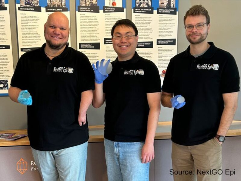
NextGO Epi has raised €2 million in pre-seed funding to expand the development and commercialisation of gallium oxide epiwafers for high voltage power electronics.
The Berlin company, which was spun out from the Leibniz Institute for Crystal Growth, produces epitaxial gallium oxide layers using metal organic chemical vapour deposition. Its current work includes wafers up to four inches in diameter for device development and customer qualification.
Gallium oxide is an ultra-wide-bandgap semiconductor with the potential to operate at high electric fields. In power devices, that property could support smaller structures, reduced conduction losses, and higher voltage operation than conventional silicon components.
Target markets include grid equipment, renewable energy inverters, electric vehicle charging, industrial power conversion, radio frequency systems, and data centre power supplies. Each is driving demand for devices capable of switching high voltages efficiently while reducing the size of cooling systems, magnetics, and surrounding passive components.
The funding will support production capability, process development, and engagement with device manufacturers. NextGO Epi will need to show that its layers can be produced with consistent thickness, composition, doping, surface condition, and defect density across the usable area of each wafer.
Epitaxy forms one of the critical manufacturing stages because device behaviour depends heavily on the quality of the deposited layer. Small variations at wafer level can create differences in breakdown voltage, leakage, yield, reliability, or switching performance after fabrication.
The company is also involved with the GOAL application laboratory at IKZ, which connects material development with practical device requirements. That environment should shorten the feedback loop between epitaxial growth, characterisation, device fabrication, and electrical testing.
Gallium oxide enters a market where silicon carbide and gallium nitride have already moved into substantial commercial production. Manufacturers are expanding those technologies through programmes including larger gallium nitride manufacturing platforms developed by ROHM and AIXTRON.
Silicon carbide is established in traction inverters, industrial drives, renewable energy systems, and high voltage conversion, while gallium nitride has gained ground in faster-switching applications at lower and medium voltage. Gallium oxide will therefore need to offer a measurable performance or cost advantage rather than relying on theoretical material properties.
Thermal management remains one of its principal limitations. Gallium oxide conducts heat less effectively than silicon carbide, which can restrict power density unless the device structure, substrate, package, and cooling system are developed as one design.
High electric field capability does not remove the heat produced through conduction and switching losses. Packaging engineers will need to move that heat away from the active region without introducing excessive electrical inductance or compromising high voltage insulation.
Device developers must also address contact resistance, controllable doping, interface quality, long-term stability, and the availability of reliable normally-off architectures. Each of those factors will influence whether the material can progress from laboratory devices into products suitable for industrial systems.
NextGO Epi has stated an ambition to support six-inch wafers at a price below €1,000 during 2027 or 2028. Reaching that target will require improvements in substrate availability, growth rate, equipment utilisation, yield, and handling, while customers will expect stable specifications across repeated deliveries rather than isolated high-quality samples.
Qualification cycles in power electronics can be lengthy because component failure may damage expensive equipment or interrupt critical infrastructure. Device manufacturers and their customers will require accelerated life testing, failure analysis, and field evidence before adopting a new material in volume programmes.
European control of epitaxial growth could nevertheless offer strategic value. Power semiconductors are becoming central to vehicles, grids, renewable generation, industrial drives, charging equipment, and computing infrastructure, placing greater emphasis on access to materials and production capability.
The €2 million round remains modest compared with the capital required for full semiconductor manufacturing, but it gives NextGO Epi the means to move from research-led supply towards a structured commercial operation. Customer device results will provide the next test of whether wafer quality remains consistent through fabrication and qualification.
Gallium oxide is unlikely to replace established materials across every power application. Its strongest opportunity will emerge in voltage and efficiency ranges where electrical performance can outweigh thermal and manufacturing disadvantages, provided wafer quality, device design, packaging, and production economics advance together.