EnSilica has secured a US$2.4 million development and supply agreement for a healthcare application-specific integrated circuit (ASIC) after completing an initial feasibility programme for a US customer. The Oxfordshire-based chip designer has separately completed tape-out of a life-sciences ASIC for a UK-listed company, advancing an existing contract valued at approximately US$1.6 million towards wafer fabrication.
The new healthcare agreement covers an expected 18-month development programme for a wireless biosensing and therapeutic controller. The end application will combine sensing and therapeutic control, with cloud-based artificial intelligence supporting treatment of a chronic condition. The customer and medical indication remain confidential. The US$2.4 million contract value covers engineering development; semiconductor supply under the product’s future commercial programme represents a separate opportunity dependent on adoption and regulatory approval.
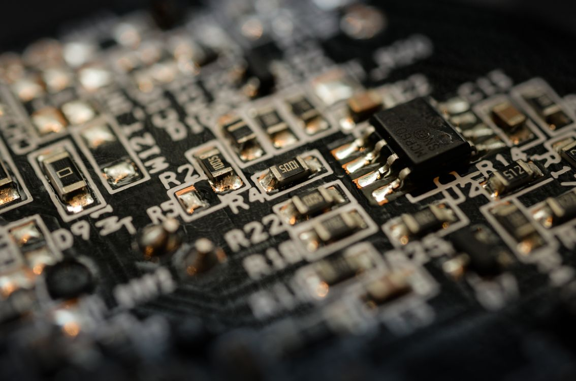
An ASIC is a semiconductor designed to perform a defined set of functions for a particular product, rather than a general-purpose processor intended to serve many applications. In a wireless medical system, the allocation of sensing, control and communication tasks to dedicated circuitry can affect power consumption, physical size and the way signals are processed. Those engineering considerations are especially important when an end product must operate with limited available power and consistent measurement behaviour.
EnSilica is developing the controller ASIC within a larger connected healthcare system. The cloud-based AI element belongs to that overall application, while the chip’s immediate engineering role is in biosensing, control and wireless functions. The final circuit architecture, semiconductor process and system operating specifications will be determined through the development programme, along with the verification requirements imposed by the customer’s product design.
EnSilica began the relationship with a funded feasibility study valued at around US$200,000. That stage assessed the customer’s requirements and the suitability of the company’s eSi-Sense healthcare platform for a full development programme. Conversion to the signed US$2.4 million agreement advances the customer relationship from technical feasibility to contracted implementation, while leaving future chip volumes dependent on the finished medical product reaching commercial use.
Moving from a feasibility assessment into design development shifts the engineering effort towards implementation, verification and manufacturability. A custom semiconductor design has to satisfy functional requirements before the final layout is committed to physical production. In medical and life-sciences equipment, the surrounding product will also need suitable system verification, with any applicable regulatory approvals and commercial production decisions determined separately from successful chip design.
The company’s separate UK life-sciences project has reached tape-out under an approximately US$1.6 million contract first identified in March. Tape-out is the point at which the completed chip layout is passed into the foundry manufacturing process. Prototype wafers can then be fabricated and evaluated against the intended electrical and functional requirements before the customer decides how to progress towards production.
Under the approximately US$1.6 million life-sciences contract, EnSilica is responsible for semiconductor design implementation, tape-out management and prototype wafer manufacturing services. The project is progressing to fabrication at an external foundry, with the company continuing to support the customer during wafer production and into later manufacturing stages. Most of the contract revenue is expected to fall within EnSilica’s financial year ending 31 May 2027.
Wafer fabrication builds the circuits through successive semiconductor processing steps before completed devices undergo electrical and functional testing. Measurements from prototype devices can prompt changes to test methods, peripheral circuitry or the system around the ASIC; some findings may require further design work. EnSilica’s completed tape-out therefore establishes an engineering milestone, with wafer results and qualification activity forming the next measurable stages.
EnSilica operates a fabless model, combining semiconductor design and technical project management with manufacturing at specialist foundries. This separates the company’s design capability from the capital-intensive facilities required to process silicon wafers. It also makes coordination of design rules, fabrication requirements, test plans and supply arrangements a material part of delivering a custom chip, particularly when the customer’s product may have a long operating life.
Both agreements create routes towards repeat semiconductor supply once their engineering milestones are completed. The US healthcare contract contains a framework for supplying the ASIC during the future product’s commercial life, while the UK life-sciences project could generate production-wafer revenue after prototype fabrication and qualification. Revenue from these prospective manufacturing phases will depend on each customer’s technical progress and demand.
The next milestones differ between the programmes. The US healthcare device will continue through an expected 18 months of ASIC development, while the UK analysis-system chip moves into prototype wafer fabrication and testing. Their combined values cover one new development contract and one existing life-sciences programme, with longer-term semiconductor sales to be determined by the customers’ subsequent product plans.