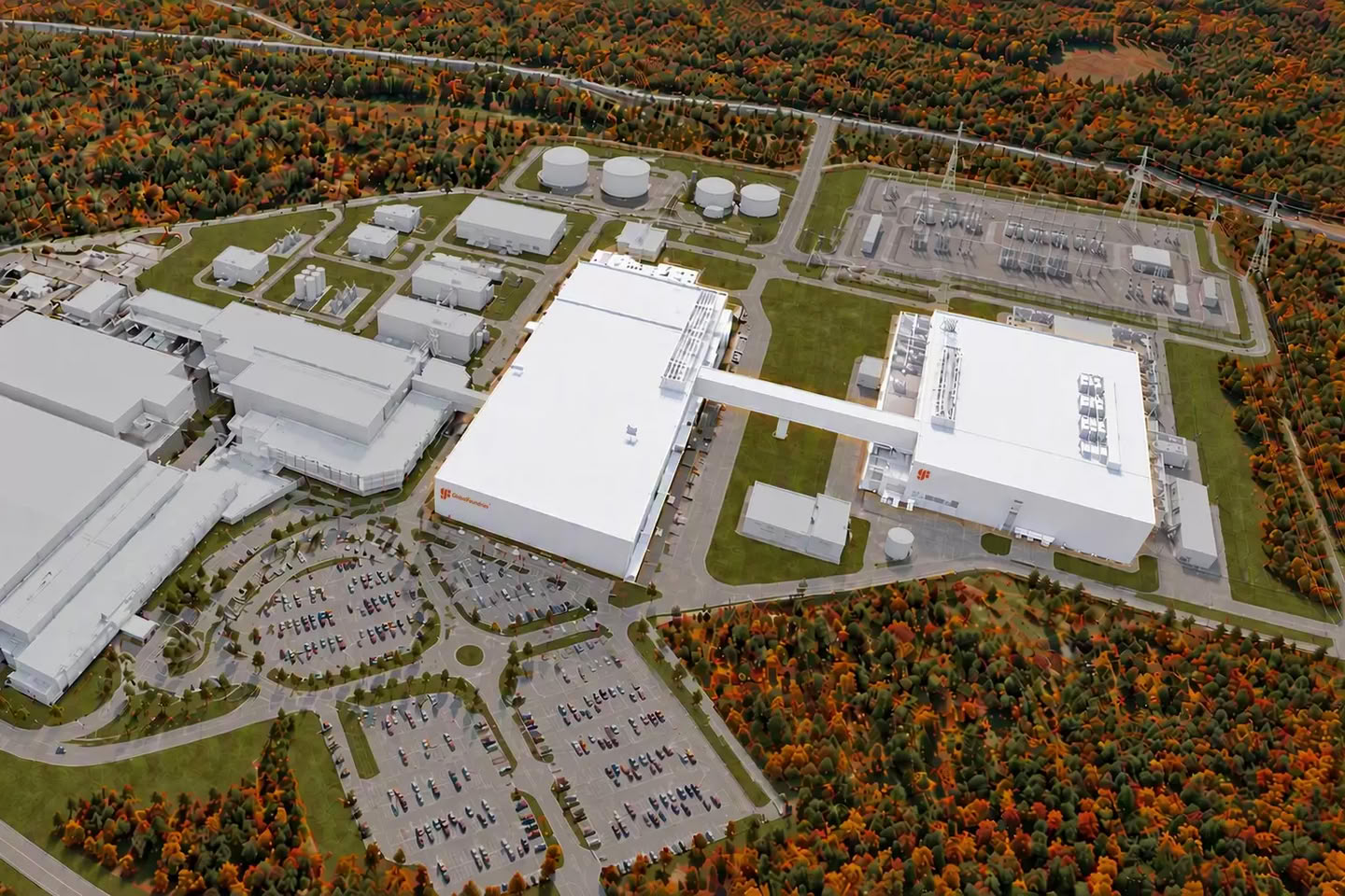
GlobalFoundries has begun constructing a new 300mm semiconductor fabrication plant at its Malta campus in New York, advancing a US–Japan manufacturing initiative from an investment agreement to physical works. Officials from both countries joined the 13 November groundbreaking. The company had been selected in October to provide technology and operate up to two proposed fabs supported by as much as $21bn in funding; the first is targeted to come online in 2029, while the second remains a separate phase subject to approval.
Approximately $10bn is associated with the first facility, alongside $570m of incentives from New York State. Japan is expected to provide the principal investment under the bilateral initiative, with GlobalFoundries supplying manufacturing technology, construction expertise and operational management. The 13 November event confirms construction has started, but does not mean semiconductor process tools are installed, validated or producing commercial wafers. Those steps will follow on a separate engineering and commissioning schedule.
At full operation, the first fab is expected to provide approximately 900,000 wafers of annual 300mm manufacturing capacity. A second plant could add a similar amount if the later phase proceeds. Capacity measured in wafers cannot be translated directly into a fixed number of saleable chips: die area, mask layout, defect density, yield and process complexity vary significantly between products. These figures are planned full-run-rate capacity, not output achieved or customer deliveries already committed.
GlobalFoundries was selected as technology provider and operator on 14 October, when the proposed programme was first disclosed. Breaking ground a month later establishes a new construction milestone and does not itself constitute another $21bn commitment. The initial phase and potential second phase have different approval and delivery dependencies. Investors and suppliers should distinguish the programme’s upper funding figure from spending completed at the site or the amount of capital equipment already ordered.
A 300mm wafer provides the substrate on which repeated semiconductor devices are fabricated. Hundreds of process operations may be necessary to create patterned layers and electrical connections, with deposition, lithography, etching, cleaning, implantation, heat treatment and metrology conducted in controlled sequences. Larger wafers can produce more dies per process cycle than smaller wafers when the design and process are comparable, but high yields require precise control of film thickness, contamination, overlay and electrical properties throughout manufacturing.
The building programme must support a complex range of utilities before processing equipment can be commissioned. Cleanroom air systems manage particles and temperature, while semiconductor tools require high-purity gases, chemicals, ultra-pure water, stable power and cooling. Waste streams and exhaust gases need dedicated handling and treatment. Factory control systems must coordinate material movement, equipment maintenance, measurement records and traceability. Tool installation, qualification and customer acceptance can continue long after construction begins.
GlobalFoundries’ existing Malta campus provides established production operations, utility corridors and engineering personnel that may support expansion. Nevertheless, a new large-scale fab requires its own environmental controls, distribution systems and tool integration programme. The company has not published a detailed schedule for each cleanroom handover, equipment installation or customer qualification stage. The announced 2029 date refers to the planned first plant entering operation, not necessarily full utilisation from its first day.
The new capacity is intended for foundational semiconductor applications in automotive, industrial and connected infrastructure products. These markets use devices for sensing, embedded control, communications and power management, often with long qualification and product-support cycles. Manufacturing suitability is not determined solely by the smallest transistor geometry; stable process performance, automotive or industrial qualification and predictable long-term supply are also relevant. The 13 November materials do not identify every process to be installed or every device that will be produced at Malta.
GlobalFoundries estimates that the two-fab initiative could support more than 1,000 skilled manufacturing jobs and about 27,000 construction and wider ecosystem jobs in New York’s Capital Region. Those projections cover the broader initiative rather than employees already recruited for the first phase. Construction contractors, mechanical and electrical specialists, process equipment installers and semiconductor suppliers would contribute at different stages. Staffing levels will depend on how the project progresses and whether the second fab is approved.
The company is separately pursuing silicon photonics, silicon-germanium and advanced packaging capabilities elsewhere in its US development programme. Those investments should not be combined indiscriminately with the two-fab figure, which describes a particular US–Japan funding arrangement. Likewise, the New York State incentive package supports the first fab but does not mean the whole sum has been drawn down or spent. Costs and capacity will be realised over several years as construction and qualification proceed.
The first facility is expected to enter operation in 2029, followed by a production ramp dependent on completed tools, demonstrated yields and customer approvals. Whether a second facility moves forward remains subject to its own decision. Subsequent construction updates and equipment commissioning milestones will provide more reliable measures of execution than the headline funding ceiling alone.