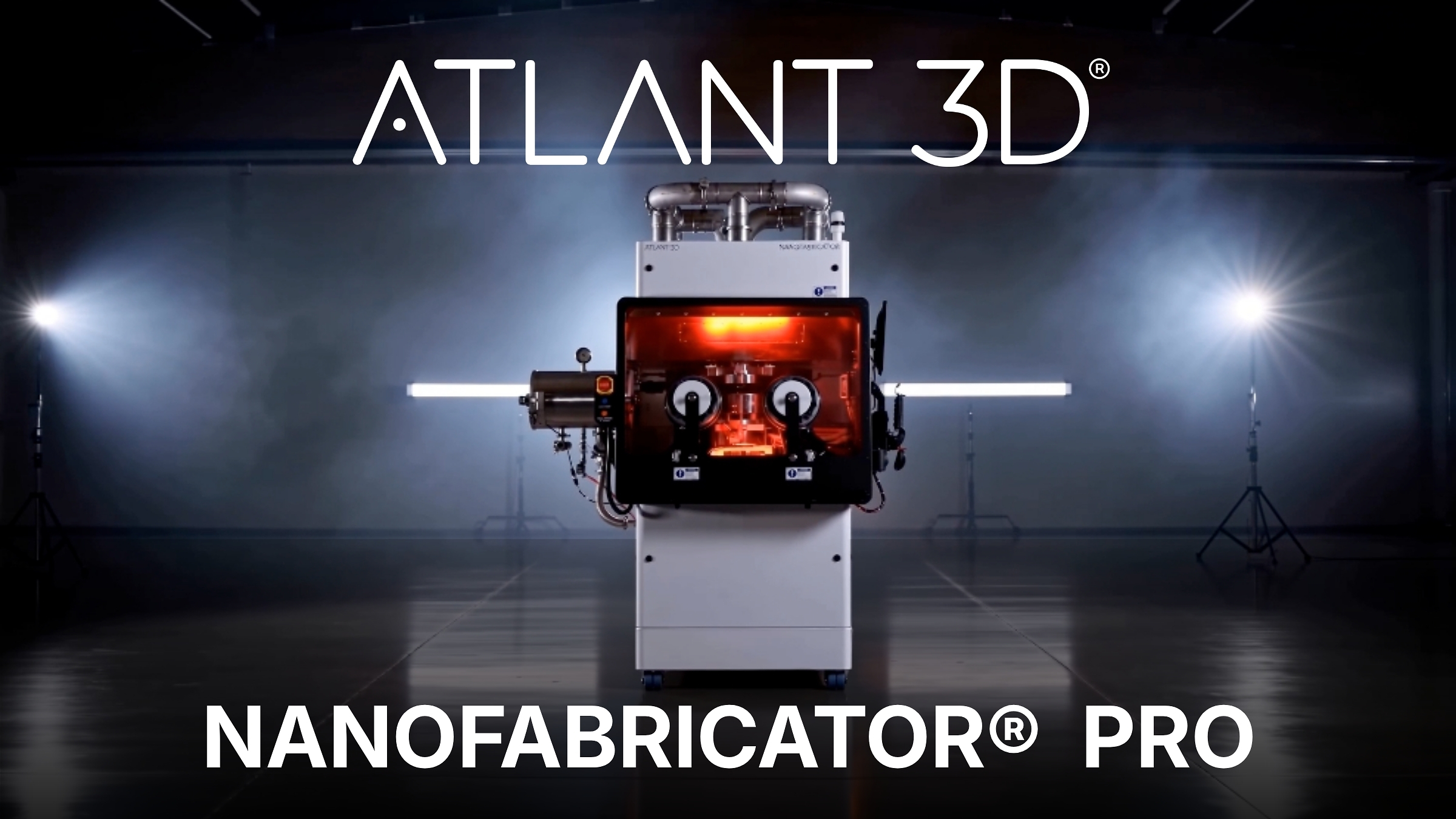
ATLANT 3D has launched NANOFABRICATOR PRO, an atomic-scale materials fabrication platform intended to connect AI-assisted materials discovery with physical deposition, experimental validation, and device prototyping. The Copenhagen-based company is positioning the system as the industrial layer of a wider autonomous materials-development architecture, with the platform aimed at semiconductor, advanced-packaging, quantum, sensor, and other research environments.
The launch addresses a practical bottleneck in computational materials development. AI systems can screen large numbers of compositions, structures, and process combinations faster than conventional laboratory programmes, but a predicted material is useful only when it can be fabricated, measured, reproduced, and incorporated into a device. Faster digital discovery therefore increases pressure on the physical laboratory to generate dependable experimental evidence at a comparable pace.
ATLANT 3D’s approach is built around Direct Atomic Layer Processing, or DALP, which adapts atomic-layer deposition into a spatially selective process. The company’s microchemical reactor deposits material locally rather than coating an entire substrate indiscriminately, allowing engineers to control where layers are formed as well as their thickness and sequence. Metals, semiconductors, and oxides can be combined through the same underlying architecture, giving researchers a route to build structures that would otherwise require several separate patterning and deposition stages.
NANOFABRICATOR PRO develops that process into a larger research and pilot-manufacturing platform. ATLANT 3D says the machine is intended for industrial R&D and low-volume manufacturing, with support for semiconductor and advanced-device work where rapid iteration matters more than high-volume wafer throughput. The company is coupling the fabrication hardware with software and automated experimental workflows rather than treating deposition as an isolated machine operation.
That broader system is central to ATLANT 3D’s longer-term A-HUB Autonomous Materials Foundry concept. The aim is to connect materials design, fabrication, experimental data, and subsequent optimisation in a tighter loop, allowing a computational model to propose an experiment, produce a physical structure, measure the result, and use those measurements to determine the next iteration. Fully self-driving materials development remains an ambition rather than a completed industrial system, but the new hardware is intended to provide the physical execution layer required for that model.
The company already has a commercial reference for the approach. In July, ATLANT 3D announced an order from an unnamed global AI hyperscaler for its smaller NANOFABRICATOR LITE platform. The customer plans to use the system in an AI-driven materials-discovery laboratory to fabricate and validate computer-generated material designs while returning experimental data to the development workflow.
That order is relevant because it tests the central proposition outside ATLANT 3D’s own laboratories. The customer is expected to use the equipment across areas including semiconductors, advanced packaging, photonics, energy technologies, and quantum systems, where new materials often fail to progress because fabrication and validation cannot keep pace with computational screening.
The engineering challenge now shifts from demonstrating unusual deposition capability to proving repeatability across a broader operating envelope. Semiconductor and advanced-device development is unforgiving of contamination, interface defects, thickness variation, poor uniformity, or unstable process conditions. A platform that accelerates experimentation still has to produce results that can be compared from run to run if the data are to be useful for either engineers or machine-learning models.
ATLANT 3D also enters a market with an extensive installed base of deposition, lithography, etch, inspection, and metrology equipment. NANOFABRICATOR PRO does not need to replace those systems to become useful. A more credible near-term role is in development environments where researchers need to create unusual material combinations or patterned structures without committing every experiment to a full conventional semiconductor process sequence.
Direct-write deposition can reduce the amount of material consumed during those experiments because only selected areas are processed, while programmable control makes it easier to generate arrays of related structures within one development campaign. That changes the economics of experimentation more than it changes the economics of high-volume wafer production, at least initially. The useful output is not merely a finished sample but a larger volume of structured physical data generated quickly enough to inform the next design cycle.
ATLANT 3D’s July hyperscaler order suggests there is already demand for that bridge between digital prediction and physical validation. The PRO platform pushes the same principle towards more demanding industrial research, where customers will expect integration with existing process controls, metrology, data systems, and laboratory routines rather than a standalone demonstration machine.
Materials AI will ultimately be judged by what survives fabrication and reaches production, not by how many plausible structures a model can propose. NANOFABRICATOR PRO gives ATLANT 3D a more substantial machine for closing that gap. Its commercial value will depend on whether customers can generate reproducible experimental evidence quickly enough to make the platform part of routine materials engineering rather than an impressive but isolated laboratory tool.