Infineon has launched its OptiMOS 7 40V switching-optimised power MOSFET portfolio for high-frequency DC-DC conversion in AI servers, data centres and telecom equipment. The devices are intended for low-voltage switching stages where electrical losses and heat removal must be managed within compact power assemblies. The manufacturer lists applications including intermediate bus conversion in 48V systems and the low-voltage secondary side of converters associated with emerging 800V DC infrastructure, with operation above 1MHz possible in suitable converter topologies.
The 40 V rating refers to the transistor’s permissible drain-source voltage, not the distribution voltage of the data centre in which the component may be used. In an 800 V architecture, lower-voltage MOSFETs can be deployed in a secondary-side conversion stage after energy has been transferred and stepped down. Intermediate bus converters for 48 V distribution provide another application. Converter topology, isolation where required and voltage transients determine which device rating is appropriate at each point in the circuit, making the distinction between the incoming bus and the MOSFET’s local switching stage essential.
Every switching cycle creates a balance between conduction and switching losses. When a MOSFET carries current, its on-state resistance contributes to heating; when it changes state, capacitances and gate-drive requirements affect the energy used during the transition. The losses become more demanding as switching frequency increases, especially in high-current circuits with limited space for cooling. Device selection therefore involves resistance and charge characteristics together, rather than treating the lowest nominal on-resistance as a complete measure of converter performance.
Infineon’s portfolio is designed around three related electrical parameters: on-state resistance RDS(on), output charge Qoss and gate charge Qg. Output charge affects the energy associated with the device’s output capacitance as the switching node voltage changes, while gate charge influences the demands on the driver. Their contribution to loss depends on topology and switching conditions. In suitable designs, reducing these burdens can help accommodate higher-frequency operation and smaller passive components, provided magnetic losses, interference and thermal limits are managed as part of the complete power stage.
A like-for-like comparison is provided for source-down device IQE010N04LM7CGSC and the OptiMOS 6 IQE013N04LM6CGSC. At 4.5 V gate-source drive, Infineon reports up to a 33% reduction in maximum RDS(on) and up to a 35% improvement in each of the output-charge and gate-charge figures of merit. These are component-level comparisons under specified test conditions, so their effect on an assembled converter will also depend on current, switching strategy, surrounding losses and cooling. The figures establish the relative device performance rather than a guaranteed reduction in a server’s electricity demand.
Richard Kuncic, Business Line Head Power Switches at Infineon, said: “With the OptiMOS 7 40 V, we give designers a MOSFET that cuts conduction and switching losses at the same time, so they can raise power density in the very limited space of an AI server.” The devices are optimised for a 5 V gate drive and intended to work within driver arrangements also used for GaN-based designs, although the parts themselves are silicon MOSFETs. Their maximum rated junction temperature is 175°C, placing a defined limit on semiconductor temperature that the system’s heat-removal design must respect.
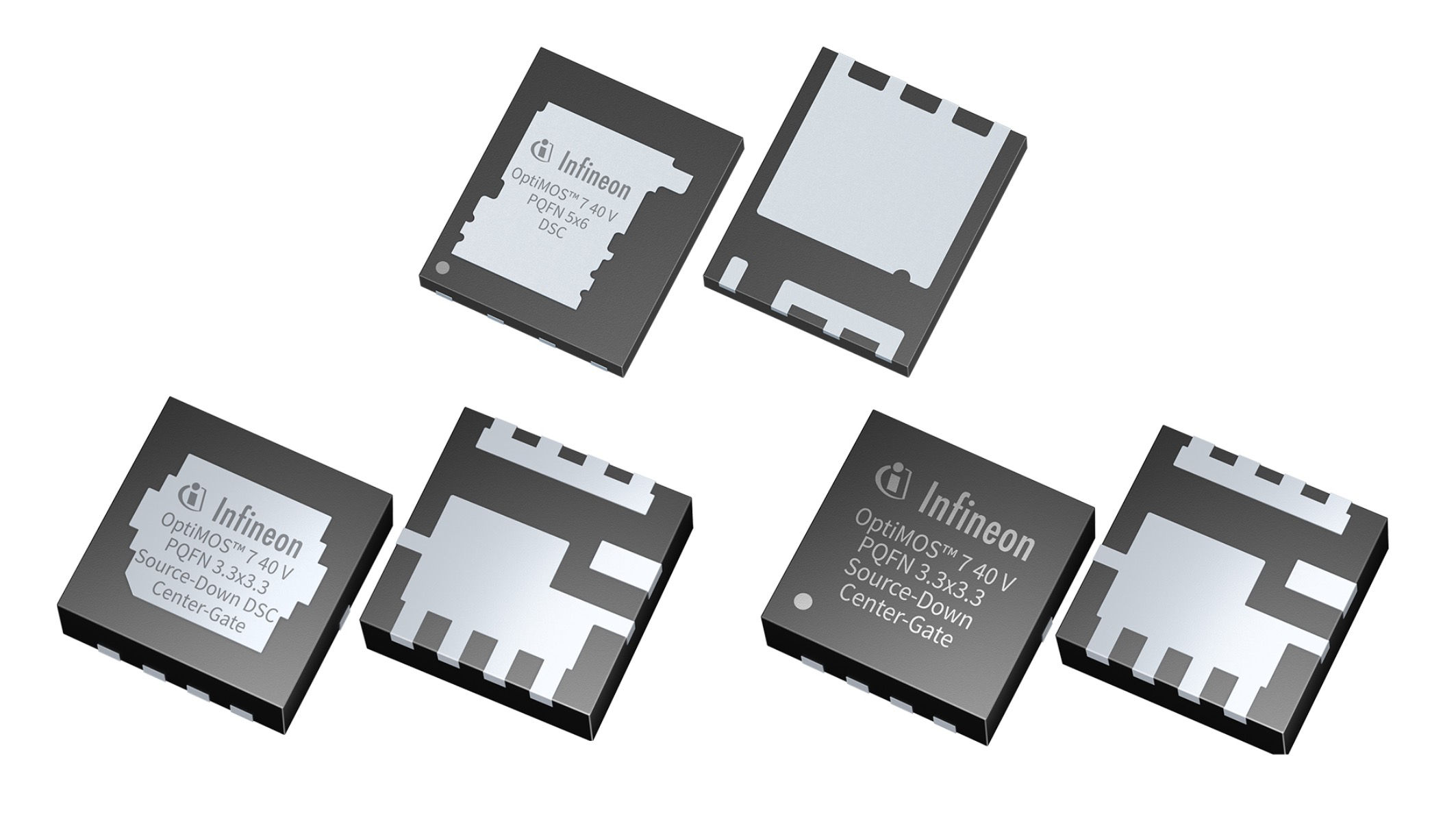
The IQE010N04LM7CG and IQE010N04LM7CGSC use PQFN 3.3 mm × 3.3 mm centre-gate, source-down packages, with overmoulded and dual-side cooling variants. Both are rated at a maximum RDS(on) of 1.0 mΩ with 10 V gate-source drive. Source-down packaging places the relevant electrical and thermal paths differently from conventional drain-down arrangements, giving layout designers another option where current density and PCB area are constrained. The dual-side cooled device provides an additional thermal interface that can be used in a suitable assembly.
Three further devices — ISCH65N04LM7SC, ISCH69N04LM7SC and ISC011N04LM7SC — come in dual-side cooled, drain-down PQFN 5 mm × 6 mm packages. Their maximum on-state resistances are 0.65 mΩ, 0.69 mΩ and 1.1 mΩ, respectively, at a 10 V gate-source voltage. The two package families offer different current-path and thermal-layout choices, while the stated resistance figures provide a consistent comparison at the same test voltage. Selecting between them also involves mechanical clearance, connection geometry and the board’s ability to remove heat.
At high switching speeds, package geometry and circuit layout influence parasitic inductance and the behaviour of current loops. Short, carefully controlled switching paths can reduce unwanted voltage overshoot and interference, while thermal interfaces and copper areas determine how heat reaches the cooling structure. Source-down and dual-side cooled packages give designers different ways to balance these demands. The benefit of any configuration has to be assessed in the actual converter assembly, where the gate driver, power devices, magnetic components and cooling hardware interact.
The portfolio supports switching frequencies above 1 MHz in suitable circuit topologies, a capability that can permit smaller magnetic and filtering components. Higher frequency also increases the number of switching events each second, so losses, electromagnetic interference and gate-drive performance need to be considered together. Devices with reduced resistance and favourable charge characteristics widen the range of possible design trade-offs, but the final frequency is set by the complete converter and its operating envelope, not by the MOSFET part number alone.
The new range is in mass production and targets AI server power delivery, intermediate bus converters and telecommunications infrastructure. Infineon provides application examples and performance benchmarks alongside the product specifications, allowing the resistance, charge and packaging options to be compared in defined circuits. Design decisions will depend on switching frequency, input and output voltage, load current and available cooling. The launch adds low-voltage switching choices for equipment moving towards denser power conversion in both 48 V and emerging 800 V distribution architectures.