In semiconductor production, high precision is essential. A critical stage is the lapping of the blanks, which ensures a uniform thickness. In order to continuously monitor the wafer thickness, white light interferometers are ideally suitable, says Glenn Wedgbrow
Many process steps are required before semiconductor chips can be made from silicon. First, slices around one millimetre thick are cut from a crystalline silicon ingot, which are then lapped. This gives them the desired thickness and surface quality. Only then can semiconductor chips be manufactured from the wafers using further processes.
Monitoring the lapping process
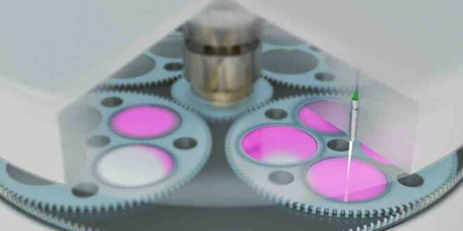
With modern lapping machines, the surfaces can be processed with extremely high precision. Silicon wafers require surface inaccuracies in the nanometre range. To machine the surface, a mixture of liquid and cutting grains is placed between the lapping disc and the wafer. Material is removed and the surface smoothed as the lapping disc and the wafers rotate against each other around different axes. The thickness of the wafer must be measured in order to achieve the required accuracy in terms of surface quality and thickness. Ideally, this happens during the process, which can then be precisely controlled on the basis of the measured values.
One measuring method that enables thickness measurements with accuracies in the nanometre range is interferometry, which is based on the wave nature of light. If two waves are superimposed, constructive interference can occur when wave crest meets wave crest or wave trough meets wave trough. Destructive interference can occur when wave crest meets wave trough.
Interferometry for industrial applications
As a metrological method, interferometry uses a light beam that is split so that the two partial beams travel different paths. The partial beams are then superimposed and the resulting interference is observed. If the length of one of the two partial beams now changes, this is visible in the interference pattern. If this length changes by half a wavelength of the light used, this leads to a complete change from constructive interference to destructive interference. If the method is to be used for thickness measurement, the two beams can interfere with each other, which is reflected by the front and back of the layer. This means that the measurement result is also independent of the distance to the measuring object.
White light interferometers
Interference works with monochromatic light, for example, from a laser. When the measured length is changed, the interference pattern alternately changes from light to dark. However, in principle, interferometry also works with white light. The only important factor is that a coherent light source is used. Superluminescent diodes (SLDs), for example, are suitable for white-light interferometry. These combine the advantages of laser diodes and conventional LEDs. SLDs have a high output power and a broad spectrum.
Micro-Epsilon offers interferometers that operate using SLDs. The light beam is split, the partial beams pass through the two paths and then interfere. For the measurement, the interfering light is first split into its spectral components and then imaged onto a sensor line that records the entire spectrum. A Fourier transform is then performed to evaluate this signal. The individual peaks in the frequency spectrum then represent constructive interference, resulting in the difference between the two paths. If the two partial beams are created by reflection on the front and back of a transparent material, the thickness can be determined to a very high accuracy.
New devices for semiconductor wafers
Micro-Epsilon has had white light interferometers in its portfolio for several years. However, the existing devices had to be fundamentally redesigned for use in wafer production. The background to this is the optical transparency of the silicon wafers, which is only high enough to be suitable for interferometry in a wavelength range around 1,100 nanometres. At these wavelengths, both undoped silicon and doped wafers provide sufficient transparency. The challenge in designing the new interferometers was selecting the right components. In addition to new SLDs with the appropriate wavelength range, new gratings and a suitable detector array had to be used that are suitable for this wavelength range. The transparency of the silicon makes it possible to measure the thickness of wafers from 0.05mm to around 1mm. As transparency decreases with doping, the maximum measurable thickness is reduced to around 0.8mm for highly doped wafers.
The white light interferometers each consist of a compact sensor and a controller, which is housed in a robust, industrial-grade housing. The active temperature control included in the controller ensures high measurement stability. Micro-Epsilon offers two different device types for use in the thickness measurement of wafers. A high degree of protection is required for integration in lapping machines so that the sensors are not affected by the mixture of liquid and cutting grains used. With this type, both the sensor and the controller unit comply with protection class IP67. However, thickness measurement can also be used in other stages of semiconductor production, for example, quality control. The conditions here are completely different: work is carried out in a cleanroom and, if necessary, in a vacuum. Micro-Epsilon offers a device with a vacuum-compatible sensor. Connection to the controller, which can be installed in a control cabinet, is made via a fibre optic cable.
Successful product launch
The new range of interferometers from Micro-Epsilon for measuring the thickness of wafers have already been extensively tested in reference projects in the semiconductor industry. Even challenging applications were mastered: in the lapping machines, the devices measure reliably even when there is liquid with the cutting grains on the wafer surface. The cleanroom variant uses Micro-Epsilon’s own cleanroom technology, which enables cleanroom-compatible packaging of the components, for example.
The IMS5420-TH white light interferometer opens up new perspectives in industrial thickness measurement of monocrystalline silicon wafers. Due to its broadband superluminescent diode (SLED), the IMS5420-TH can be used for undoped, doped and highly doped SI wafers. In wafer thickness measurements, the IMS5420-TH impresses with an excellent price/performance ratio.
The white light interferometer achieves a signal stability in the sub-micrometer range. The thickness can be measured from a distance of 24mm. The measuring system is therefore ideally suited for inline measurements.
The measuring system is available as a thickness measuring system or as a multi-peak thickness measuring system. The multi-peak system measures thicknesses of up to five layers, for example, wafer thickness, air gap, films and coatings.
In addition to silicon wafers, the IMS5420 also precisely detects the thickness of silicon carbide wafers. For thickness measurements in harsh environmental conditions, the IMS5420/IP67 controller is available with IP67 protection and stainless steel housing.
Glenn Wedgbrow is Business Development Manager at Micro-Epsilon UK.


