Defect of the Month with Bob Willis – Solder Skips
Hello, my name’s Bob Willis and welcome to Defect of the Month. Every month, I try and provide an example of a particular defect and hopefully some solutions. And I’ve made over a hundred different defect videos over the years. So hopefully one will solve one of your problems. Remember that if you like this video content, please subscribe to the channel. If you like this individual video, then just like it. And of course, please share it with some of your other engineering colleagues within your company.
Wave solder skips, or skipping. Sometimes some people refer to this as insufficient solder where there is no solder on one joint or two joints on a board after the wave soldering process. But really there is a difference between no solder and insufficient, insufficient means there’s not enough. So there’s obviously something there anyway. So skips or skipping can occur on products that are wave soldered, particularly when we’re talking about surface mount components that are bonded to the surface of the under surface of the board using adhesive and soldered during passing the board through the wave soldering process, possibly as part of a mixed technology design.


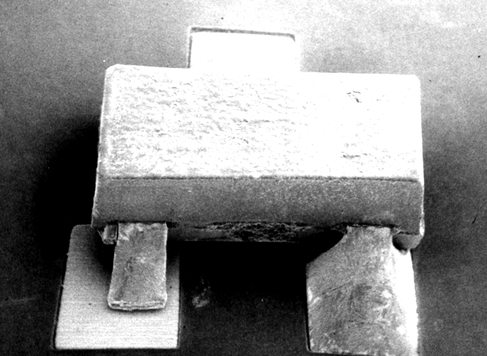
When we say skipping, we’re talking about any pads or in fact, in some cases, test pads that have no solder present. So you might find that on chip components. SOT23, SOTIC’s that have been through the soldering process, there’s a few pins with no solder on, or there is no solder on the pads. It’s important to look in detail where the solder is or isn’t because that can give you an indication of what the problem might be. So one of the reasons is incorrect pad design, if there isn’t sufficient area for the solder to wet, as the board goes through the process, then again, a joint may not be visible.
You might get an situation where there’s a difference in solderability or wettability on the surface of the pad coating that you’ve selected for your PCBs. So again, really, truly speaking, this should be a random problem across the whole of the board. But if you see skipping on soldered joints on just certain components, then it’s perhaps more likely to be related to the design of the pads on that particular part/component.
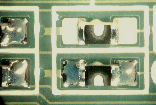
Now, if we look at what we would normally wave solder in terms of SMT, there would be chip components, SOIC’S, possibly QFPS, but less likely today. But also SOT23. Now as an indicator to me, when the process is going or drifting out of control, if I’ve got boards that has SOIC, SOT23 and chip components, the first component, which is going to give me a problem when the process is changing, going out of control, or some of the factor is coming into play, it’ll be the SOT23. So those are the ones that will show you the skips first, and then you’ll see it on other parts. So if we then start to think about, you know, what is a contributing factor? Well, I’ve already said to the pad size, but also the solar mask, the solder mask aperture opening and the mask thickness. Now very rarely do any design engineers actually specify the mask thickness requirement and the variability of the solar mask on the surface of a printed circuit board.
So if you can imagine if you’ve got a pad and you’ve got mask around it, and that mask increases in size i.e thickness that you’re actually creating a barrier around the pad, which makes it difficult for the solder to actually wet the termination, as well as the pad, also with very thick mask or variations across the printed circuit board surface that you are processing. Flux can actually sit within the cavity, which is turned upside down. So you’ve got a bucket around the termination you’re trying to solder. Volatile material can actually gas out from that surface because the flux cannot be displaced very easily from the surface of the board. So something to look out for excessive flux to start off with, if you put too much flux on, you’ve got to dry it off, evaporate the solvent carrier as part of your preheating process.
Thank you very much for listening to defect of the month. Hopefully it’s been useful and possibly you’ve found a solution to one of your process problems. So just a reminder that if you want to listen to more defect of the month, subscribe to our channel, if you just like this individual video, then please like it. And of course share it with some of your colleagues in manufacture and in other companies, it all helps to bring information to both production and engineering staff. If this short introduction to this particular problem was of interest to you, then of course we can hopefully provide you a solution to aid. You eliminate more process defects within the future. Finally, if you’ve got a defect and you’d like it covered in a future defect of the month, then let us know. Thank you very much.


