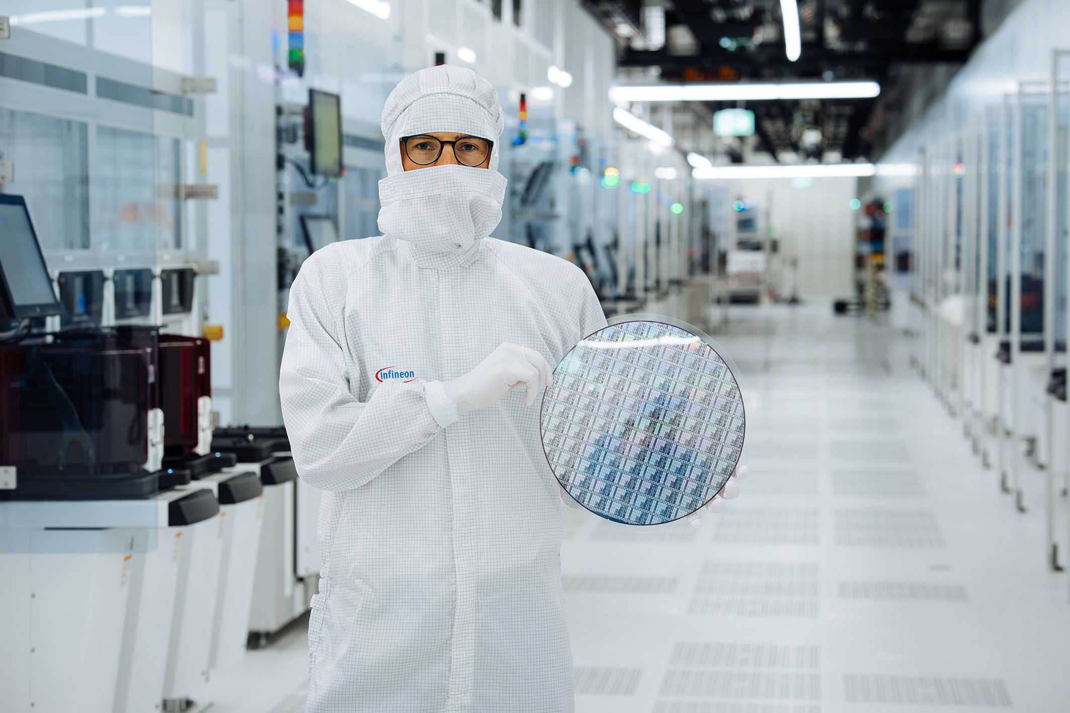
Infineon Technologies plans to invest approximately €1.1 billion in gallium nitride power semiconductor manufacturing at Villach in Austria, expanding its existing industrial site to produce devices on 300mm wafers at high volume.
Production is scheduled to begin by the end of 2027, with the overall investment programme extending to 2034. Infineon intends to use established cleanroom space and upgraded infrastructure rather than building an entirely separate semiconductor campus.
The company describes the proposed operation as the world’s first high-volume facility for gallium nitride power semiconductors manufactured on 300mm wafers. That world-first designation is Infineon’s assessment of its commercial production plans; the volume operation has not yet entered service.
The project is supported by €319 million of public funding under the European Chips Act arrangements. This figure forms part of the project’s financing context and should not be added to the €1.1 billion investment as if it were another manufacturing commitment.
Villach is already a major Infineon production and research centre for power electronics. Infineon Austria employs around 5,800 people, of whom approximately 4,800 work at the Villach location, according to the company’s latest announcement.
The investment is intended to address demand for efficient power conversion devices used in data centres, electrical infrastructure, electric mobility and robotics. These markets have different technical requirements, but all involve controlling or converting electrical energy using semiconductor switching devices.
Gallium nitride, generally abbreviated to GaN, is a compound semiconductor material that can support devices with fast switching characteristics. In appropriate circuit designs, its performance can reduce some losses associated with repeated switching between conducting and non-conducting states.
Those losses are one contribution to the efficiency of a complete power converter. Conduction resistance, magnetic components, control arrangements, wiring and cooling systems also affect how much electrical energy is lost as heat.
A faster-switching device can allow a converter to operate at a higher frequency, potentially reducing the size of transformers, inductors and other passive components. Designers must nevertheless account for electromagnetic interference, thermal conditions and switching transients when selecting operating frequencies.
The advantages therefore depend on the complete circuit rather than the semiconductor material alone. A device that performs well under one voltage, current and load profile may not offer the same system-level improvement in another application.
The manufacturing change at Villach concerns wafer diameter as well as device technology. Infineon demonstrated the processing of 300mm GaN wafers in 2024 and now intends to establish repeatable production processes at commercial volume.
A 300mm wafer has approximately 2.25 times the circular surface area of a 200mm wafer. Infineon estimates that its larger-wafer approach can deliver approximately 2.3 times as many chips per wafer compared with conventional 200mm processing.
That estimate should not be read as a corresponding improvement in final production yield or cost per approved device. The number of saleable chips depends on the geometry of individual devices, usable wafer area, process defects and results from electrical testing.
Transferring a semiconductor process to a larger substrate requires control of manufacturing conditions across a wider area. Variations in deposited layers, material properties and processing uniformity can influence the electrical characteristics of devices produced at different positions on the wafer.
The equipment used to process and inspect the larger wafers must be compatible with the substrate size and meet the tolerances required by the product. Manufacturing yield must then be established through repeated production, rather than inferred from a single successful demonstration.
Process integration creates additional demands. A power semiconductor may pass through multiple steps involving layer formation, patterning, etching, metallisation and electrical inspection. Changes to one stage can influence the performance or reliability of the completed product.
A high-volume plant must also manage the movement of wafers through these steps with consistent identification and traceability. Process records are necessary for investigating deviations, assessing quality and demonstrating that finished devices satisfy the applicable specifications.
Infineon expects the investment to support a demand-led expansion rather than immediate production at an announced maximum annual capacity. The company has not disclosed the number of wafers it intends to process each year at the completed Villach facility.
Using existing cleanroom areas could reduce the need for some building work, but specialised tools, utilities and process support systems still need to be installed and qualified. Semiconductor manufacturing requires controlled environments and reliable supporting infrastructure to maintain process stability.
GaN components are relevant to AI data centres, where electrical power passes through several conversion stages before reaching computing equipment. Improvements in the efficiency of an individual conversion stage can reduce heat generation, although the impact on total site energy use depends on the complete power architecture and operating load.
Electric mobility and robotics present other design constraints, including changing loads, package size, vibration, thermal cycling and reliability expectations. Their use of GaN will depend on whether suitably rated devices and circuits meet the requirements of each system.
The expansion also has an industrial policy dimension. European chip manufacturing depends on specialised equipment, materials and international supply networks, and adding capacity in Austria increases the regional production options available for certain power devices.
Public support under the European Chips Act is intended to strengthen semiconductor production capability, but the presence of the grant does not guarantee future sales or eliminate upstream material dependencies.
Infineon cites a projected global market of approximately US$3.5 billion for GaN power semiconductors by 2031. This is a forward market estimate, not contracted revenue from the planned Villach operation.
The immediate engineering work concerns installing and validating equipment, establishing manufacturing repeatability and preparing the 300mm process for commercial output. Production beginning by the end of 2027 would mark the initial operating milestone, while the wider investment and any demand-led capacity additions continue towards 2034.