By Bob Willis
Hello, my name is Bob Willis and welcome to Defect of the Month with WNIE. Here is another video to watch and short article with photographic examples to add to your collection of training material and help your team understand process and product failures
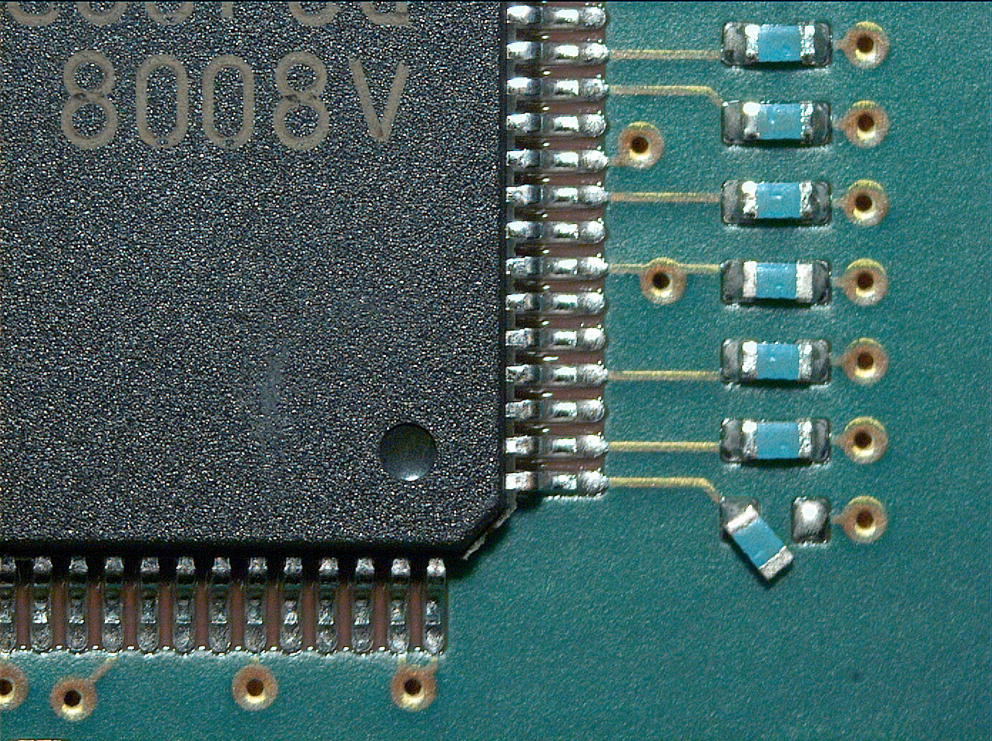
Now, it’s not uncommon to have components move during the assembly process, and one of the benefits we have today is the use of AOI, Automatic Optical Inspection, which we can introduce after placement or after soldering to make sure the components are positioned correctly, they’re in the right position.


Example of misplaced components on solder paste and a part found misplaced after soldering. The root cause needs to be investigated to improve the yield
Now if we have components that are actually spat out, poorly placed for a variety of different reasons, it might be feeders, it might be components held up in the blister tape as they’re separating away due to static. The vacuum pickup may not be sufficient to hold that part in place on the nozzle and then be placed accurately on the printed circuit board.
It could be vibration of the board during the placement process where the solder paste is not as tacky as it should be, or the print volume is poor. Poor paste print deposits can lead to misplacement. Where parts are to be held in place with adhesive for wave soldering can be lost when the adhesive volume varies
Now if these components are misplaced, we will have to look at rework in the future. Possibly adding parts as a second stage assembly. In some case like automotive industry strangely partly assembled boards can be scraped due to one misplaced part. However, they may be misplaced to such a degree they’re actually present underneath components and classic examples of this might be chip components. Small chips like 0201 under area array packages may be sufficient to hold the parts slightly off the surface of the board as shown below. These may lead to open circuit joints which are quite difficult to detect. However, they’re very easy to detect using X-ray inspection.


Two example of misplaced chip components under Ball Grid Array packages. The first x-ray image shows 0201 chip resistors which are located between the terminations. The second shows a chip capacitor soldered between two balls
Fortunately, with AOI we now have the ability on some systems to also measure variations in height of a package and we’ve used this technique to look at voiding volume in the past. We’ve also looked to use the technique to check the amount of warpage of packages however not all AOI systems have this capability, but a number of them do, so it’s a very useful tool for misplaced components underneath packages. Some engineers have used AOI for components warp during the soldering process and movement for other reasons. So look very carefully how often you get misplaced parts and also what are the root causes of misplaced components many placement systems had very good data collection and obviously AOI is a great data generator

The x-ray example above shows an area array package placed on to solder paste. It is not aligned with the paste deposit or pads and may have been misplaced or has moved due to vibration/shock movement of the board before soldering
We have many other Defect of The Month videos and our WNIE online articles which we hope will help you solve your process and product failures. We have also listed a small selection from over 100 plus videos below created over many years with NPL and IPC
BGA popcorning
Dendrite formation
Open solder joints
Solder skips
Coating bubbles
Ultrasonic damage
Missing components
Incomplete past print
Component cracking
Tombstone chips
Solder balls
Solder bead formation
Solder shorts
Sulphur corrosion
Crimp connection failures
The list goes on and on, one month at a time
If you would like to download any of our Process Defect Guides or my three soldering books FREE just drop me an email. That is also the case the Wetting Indicator procedure bob@bobwillis.co.uk


